


595 series shift registers come in many flavors. SN74HC595 is the most usual.
There are many ways to drive multiple LEDs, which in sum would require more IO pins and more current than is available on the control chip. The simplest way is perhaps multiplexing, and in this example I’ve used two 8 bits serial-in/parallel-out shift registers to achieve that. I’ll skip the theory for now, but I think the structure and layout of the LED matrix is worth highlighting.
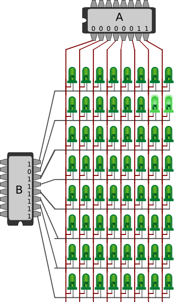
Below the 64 LEDs are shown in a grid of 8 columns and 8 rows. To light a specific LED, there has to be a potential difference between its two pins, thus the pin connected to a column should be set HIGH, and the other row pin to LOW. To individually control all the LEDs, the active row is cycled very quickly. For each step of the cycle, the specific LEDs of that row is set, and then changed for the next row. If done quickly enough (typically at least 50 times per second; 50 Hz), it will appear as if all the LEDs are always on.
The example in the figure shows register A set to 0000 0011, for the two right-most LEDs. Register B is set to 1011 1111, thus activating the second row from the top. In theory, the settings of the two registers could have been reversed, and then the two bottom LEDs of the second column had been lit. However, since LEDs are directional, and does not let current through when the polarity is reversed, this is not possible (at least not with the simple diagram shown below).
So that makes for 16 potentially different bits of information. However, as the title suggest, there’s one more available: It’s the output pin, typically used to daisy chain multiple shift register chips together. Even though it is part of the internal shift register, which thus consists of 9 bits, it is externally visible, and retains its state after the latch is closed. The drawing below shows this, with nine yellow external dots indicating visible bits, and eight blue dots indicating internal bits, for a total of 17 bits.
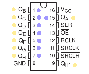
In the figure I’ve marked the QH’ as externally visible, even though it is part of the internal shift register. There probably aren’t many applications in which you’d use that as an active output, but one that comes to mind is a 3x3x3 LED cube. In a typical setup, you’d have three layers of 9 LEDs, for 12 wires altogether. Instead of controlling each LED in a layer individually, you could use a shift register, however you’d be one pin short (or 7 pins wasted if using two chips). So why not use the output pin for the 9th LED?
The programming would work as normally when addressing a shift register, but instead of shifting out 8 bits, you’d shift 9. The only problem would be that the 9th LED connected to the output pin would see the previous bits flying past as new bits are shifted onto the register. This might not be a big problem, as cycling the layers will probably be too fast to notice. If it is an issue, one could just disable all layers while bits are shifted out, and turn on only the relevant layer when done.
// Digital pins for two independent shift registers.
const int dataA =  5;
const int latchA = 6;
const int clockA = 7;

const int dataB =  8;
const int latchB = 9;
const int clockB = 10;

const int outputPinCount = 6;
const int outputPins[outputPinCount] = {
  dataA, clockA, latchA, dataB, clockB, latchB};

// Frame buffer
const int lights = 64;
int buf[lights];

void setupPins() {
  for (int i = 0; i < outputPinCount; i++) {
    pinMode(outputPins[i], OUTPUT);
  }
  clearAll();
}

void setup() {
  Serial.begin(9600);
  Serial.println("reset");

  setupPins();
  setAll(1);
}

void loop() {
  display();
}

void clearAll() {
  setAll(0);
}

void setAll(int v) {
  for (int i = 0; i < lights; i++) {
    buf[i] = v;
  }
}

void display() {
  for(int grp = 0; grp < 8; grp++) {
    digitalWrite(latchB, LOW);

    // Writes a single bit to the B register.
    // 0 means that group is active / on, 1 means off.
    // At the beginning of the loop, one 0 is shifted
    // onto the first bit, and later shifted upwards
    // as 1s turn the previous groups off.
    digitalWrite(clockB, LOW);
    digitalWrite(dataB, grp == 0 ? 0 : 1);
    digitalWrite(clockB, HIGH);
    digitalWrite(latchA, LOW);

    // Depending on the arrangement of the LEDs, and which
    // bits are conceptually most/least significant, shift in
    // increasing or reverse order.
    for(int i = 7; i > -1; i--) {
      digitalWrite(clockA, LOW);

      int bit = buf[grp * 8 + i];
      digitalWrite(dataA, bit);

      digitalWrite(clockA, HIGH);
    }

    // Here and above, both latches are set to the same
    // value at the same time, this could have been combined
    // onto the same IO pin.
    digitalWrite(latchA, HIGH);
    digitalWrite(latchB, HIGH);
  }
}
Shift register is controlled with three pins. They are usually called DATA, LATCH and CLOCK. Chip manufacturers have different names. See the table below for two examples from Texas Instruments.
| 74HC595 | TPIC6B595 | |
|---|---|---|
| DATA | SER | SER IN |
| LATCH | RCLK | RCK |
| CLOCK | SRCLK | SRCK |
CLOCK is an constant high – low signal used to synchronize data transfer. Each time CLOCK
goes high two things happen. Current value in shift register gets
shifted left by one. Last bit is dropped out. First bit will be set to
current value of DATA. To write a byte to shift register this has to happen eight times in a loop.
End Of Post